Tesla charts path to 80X performance gains with rebranded SI accelerator lineup
The automaker has unveiled its next-generation AI chip roadmap, swapping the AI designation for SI terminology while detailing plans for a radical redesign of its Dojo training processor and massive leaps in inference performance through 2030.
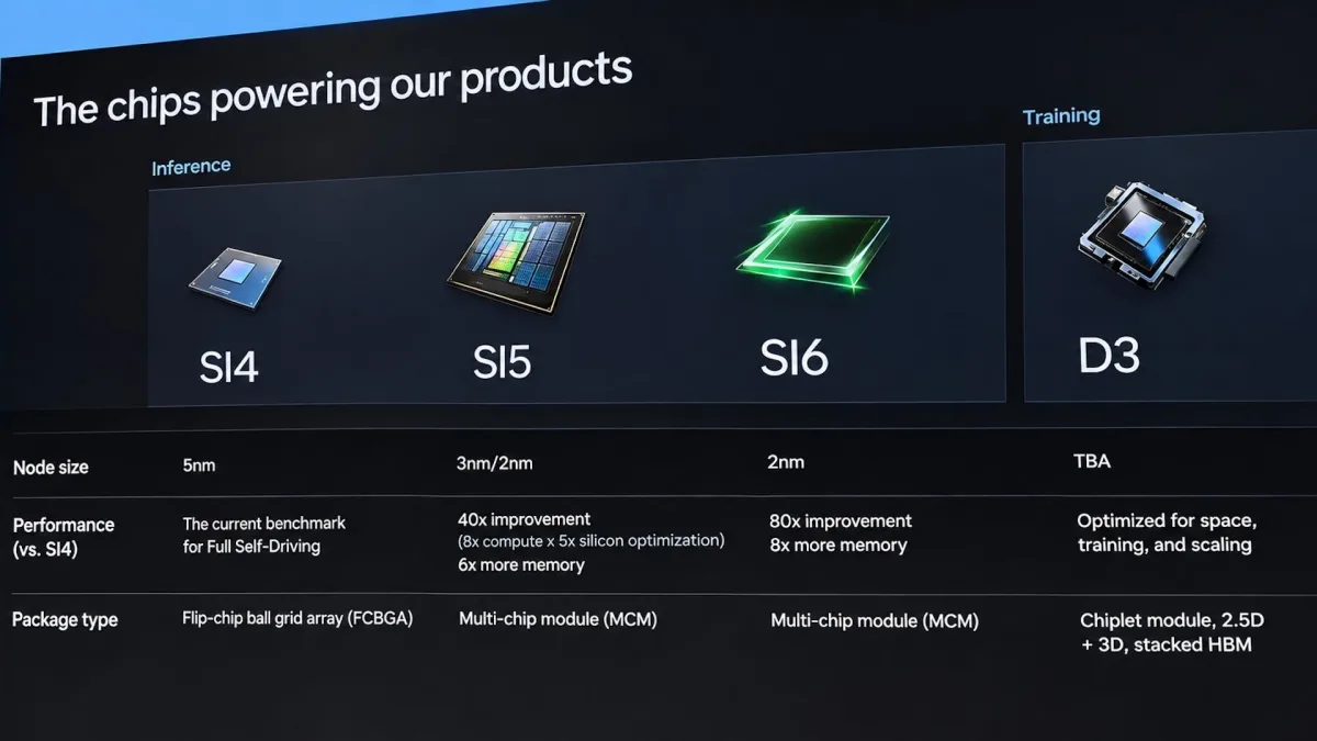
Tesla's custom silicon strategy is taking shape with a refreshed accelerator roadmap that signals major shifts in the company's chip architecture and naming conventions. The Elon Musk-led firm has rebranded its AI accelerators under the "super intelligence" banner, moving from AI4, AI5, and AI6 designations to SI4, SI5, and SI6 respectively. The 6th Generation inference accelerator will deliver 80 times the compute performance of the current 4th Generation chip, while the company's revived Dojo D3 training accelerator abandons the SRAM-centric design of earlier generations in favor of a multi-chiplet approach with stacked HBM memory.
Wait a minute… I thought @elonmusk 's Tesla chips were called AI4, AI5, and AI6. But in this latest presentation, they're now labeled SI4, SI5, and SI6. Then I remembered: President Trump wants to replace "Artificial Intelligence" (AI) with "Super Intelligence" (SI). Looks like Elon Musk may already be embracing the new terminology. 🤔
Posted November 4, 2026
Musk has confirmed that SpaceX's AI division will also adopt the SI branding, becoming SpaceXSI as part of this broader terminology shift across the company's operations.
Dojo D3: A departure from wafer-scale integration
The reemergence of Tesla's in-house Dojo training accelerator marks a notable reversal after Musk cancelled the entire wafer-level Dojo project in August 2025. The company subsequently announced in August 2026 that SpaceX and xAI would rely exclusively on Nvidia hardware for both terrestrial and orbital data centers. The third-generation Dojo will differ substantially from its predecessors, Dojo D1 and D2.
Tesla characterizes the D3 as a chiplet-based design combining 2.5D and 3D packaging with stacked HBM, a significant departure from the original Dojo D1 system-on-wafer architecture. The D1 relied on distributed on-chip SRAM and interconnected 25 D1 processors with 11 GB of SRAM using wafer-scale packaging. The shift to HBM reflects Tesla's need to substantially expand memory capacity, as contemporary AI models demand enormous amounts of memory for storing parameters, activations, and intermediate computations, making SRAM insufficient from a capacity perspective. HBM simplifies memory scaling but introduces different tradeoffs in latency, bandwidth, packaging, and power consumption.
Whether Tesla has fully abandoned wafer-scale integration remains uncertain. While custom HBM modules could theoretically stack atop logic dies interconnected using wafer-scale packaging, the added complexity makes this approach less probable for D3. Stacking HBM on wafer-scale interconnected logic introduces design complications, cooling challenges, manufacturing hurdles that could reduce yields, and long-term reliability concerns—all driving up costs. The company has not yet disclosed D3's compute performance, memory capacity, manufacturing process, or development timeline.
Tesla states that Dojo D3 will be optimized for "space, training, and scaling," suggesting a more conventional accelerator architecture rather than wafer-scale packaging. The unit is also designed for extraterrestrial deployment, likely incorporating radiation hardening for select SKUs.
SI6: Pursuing 80X gains over current hardware
Tesla's roadmap discloses that the 6th Generation inference accelerator (SI6) will achieve 80 times the compute improvement over HW4 and nine times more memory. This translates to approximately 17,280 to 46,080 TOPS (trillion operations per second), or 17.28 to 46.08 POPS (quadrillion operations per second), though the data formats SI6 will support remain undisclosed. For context, Nvidia's Rubin GPU delivers 50 NVFP4 PFLOPS for inference and 35 NVFP4 PFLOPS for training, with 17.5 FP8/FP6 PFLOPS available. Rubin is shipping to customers now, whereas SI6 is targeted for 2029 to 2030.
Tesla's current 4th Generation inference processor, deployed in the company's vehicles today and previously called HW4 before being renamed AI4 and then SI4, is manufactured by Samsung Foundry using its 7nm-class process and conventional flip-chip ball grid array (FCBGA) packaging with approximately 16 GB of GDDR6 memory. Tesla uses this processor as the benchmark for its Full Self-Driving (FSD) technology. The company does not officially disclose the chip's absolute compute performance, memory capacity, or power consumption. Musk previously stated that HW4 is 3 to 8 times more powerful than HW3, which was officially rated at 72 TOPS, suggesting HW4 delivers between 216 and 576 TOPS.
The 5th Generation inference accelerator, designated SI5 (also known as HW5 or AI5), will be manufactured at TSMC and Samsung Foundry using 3nm- and 2nm-class process technologies respectively, employing a multi-chip module (MCM) design that departs from HW4's conventional packaging. Tesla expects SI5 to deliver 40 times the performance improvement over HW4, comprising an eightfold increase in compute capabilities from denser process technologies and additional execution units, plus a fivefold gain from silicon optimization. This points to approximately 8,640 to 23,040 TOPS depending on how HW4 performance is calculated. Power consumption is projected between 250W and 800W depending on application, and the processor will feature six times more memory than its predecessor—96 GB. Memory bandwidth could range from 768 GB/s to 1.536 GB/s depending on whether GDDR6 or GDDR7 is used.
The SI6 will push compute performance to 80 times that of HW4 while featuring eight times more memory than the current generation. This could yield 17.28 to 46.08 POPS, depending on how HW4 performance is measured, along with 144 GB of memory—substantial figures for an AI accelerator.
Tesla has secured a deal with Samsung Foundry to manufacture its 6th Generation inference accelerators through 2033. The new roadmap reveals the unit will use a 2nm-class process technology. Given the 2029 to 2030 target and Samsung's updated foundry roadmap, the company is likely targeting automotive-grade SF2A, performance-enhanced SF2P, or SF2Z with backside power delivery. Notably, Tesla does not plan to produce SI6 at Terafab using Intel's 14A fabrication process in the 2030s.
SI6 will maintain the multi-chip module approach introduced with SI5, a rational choice that allows Tesla to build on experience gained with the 5th Generation accelerator while keeping packaging costs reasonable. Many automakers are considering multi-chiplet designs and HBM memory for their next-generation system-in-packages, which will drive costs across the industry. The timing of Tesla's adoption of HBM for inference accelerators remains unclear, but it is unlikely to occur with SI6.