Gelsinger-Backed Nagare Labs Unveils Z2RAM, Stacked Memory Targeting AI Chip Bandwidth Bottleneck
A Georgia Tech spinout backed by former Intel CEO Pat Gelsinger is developing Z2RAM, a capacitorless memory designed to deliver SRAM performance at DRAM density directly atop AI accelerators, addressing a critical bandwidth constraint in modern chip design.
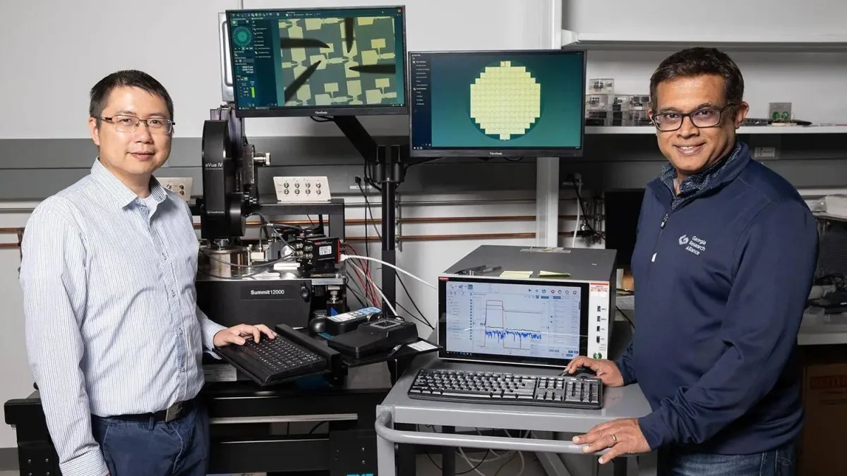
Nagare Labs, a startup emerging from Georgia Tech and supported by Playground Global, claims its Z2RAM technology can deliver memory with SRAM-class speed while maintaining DRAM-level density, stacking directly onto AI processors. According to the founders' research papers, the technology has been tested up to 85 degrees Celsius and retains data for more than 300 seconds. The first generation is projected to achieve 5x SRAM density using six stacked layers, deliver 14x the speed of DRAM, and consume 3x less read energy than SRAM.
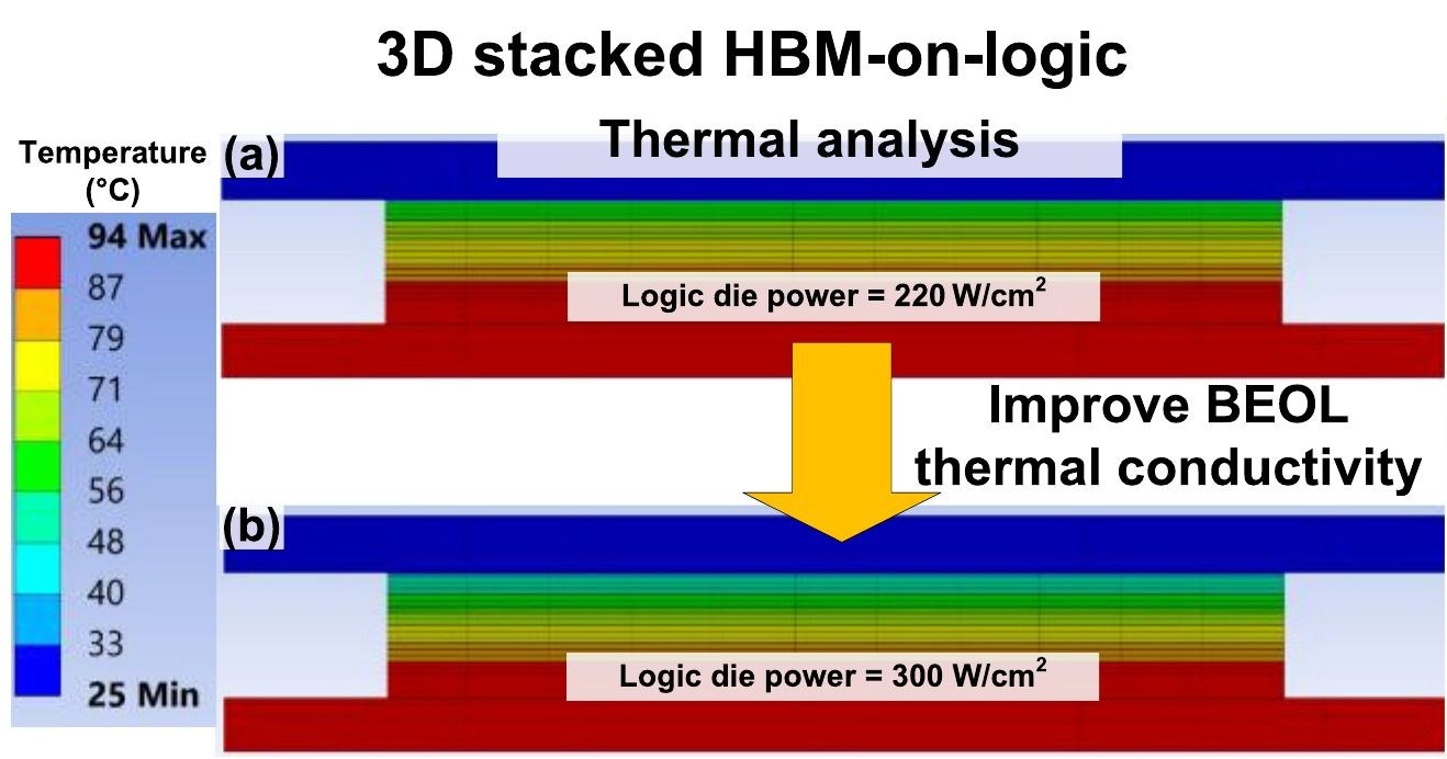
The memory industry faces mounting pressure to supply sufficient high-bandwidth memory (HBM) for AI chips, which demand enormous data throughput. Yield challenges plague HBM production, and thermal constraints limit how many layers manufacturers can stack. Samsung's zHBM, which places DRAM directly on processors, is planned for only approximately four layers due to heat concerns. DRAM stacked on compute logic faces a hard ceiling: the underlying logic cannot exceed 220 W/cm² of heat output, or 300 W/cm² with improved thermal vias, according to a 2025 simulation by co-founder Shimeng Yu's research group.
Other approaches exist but carry trade-offs. High-bandwidth flash, still under development, would stack NAND alongside the GPU. SRAM stacked directly on the die offers speed but sacrifices density and raises costs. The fundamental problem: peak compute has grown 70% annually over three decades, while memory bandwidth has advanced only 20% per year.
How Z2RAM Works
Nagare describes Z2RAM as "Two transistors and a shield. No capacitor." A write transistor deposits charge on a storage node while the shield prevents interference from neighboring cells. The read transistor can detect the charge without depleting it. This gain-cell design allows non-destructive reads and eliminates DRAM's write-back penalty. The company targets energy consumption well under a picojoule per bit.
The manufacturing process differs fundamentally from conventional stacking. Nagare deposits layers atop the accelerator and patterns them "together on one die," mirroring how 3D NAND flash scales by adding layers. No interposer exists, and memory layers bond directly to the compute die. A single lithography exposure covers multiple layers simultaneously, and standard 300 mm tools using deep ultraviolet light handle the work—no extreme ultraviolet lithography required. The current roadmap targets over 100 layers with "hundreds of thousands" of vertical connections.
The Retention Challenge
Maintaining data integrity at elevated temperatures remains the central engineering hurdle. A 2020 paper from co-founder Suman Datta's group demonstrated a tungsten-doped indium oxide two-transistor cell with 1 second retention at 25 degrees Celsius but only 300 milliseconds at 85°C. A 2025 update, with Datta as co-author, introduced a third transistor and removed gate overlap, achieving over 1,000 seconds at 25°C—up from 200 seconds with overlapped transistors. Simulation showed a GPU L2 cache matching twice SRAM's capacity in the same area while consuming 75–80% lower energy-delay-area product.
Six months later, both founders presented a "folded asymmetric boosted" three-transistor cell retaining data for over 300 seconds at 85°C, compared to only 100 milliseconds for conventional three-transistor designs. This cell operates "refresh-free," meaning data in a GPU's last-level cache, profiled from AI workloads, decays before overwriting occurs. However, neither the published cells nor Z2RAM have yet demonstrated retention above approximately 95°C, the threshold DRAM must observe.
Density and Area Projections
The founders project their boosted cell at 0.0168 µm² using 7nm technology, versus 0.0199 µm² for a high-density SRAM cell on TSMC's 3nm process. A separate study from Yu's group found that a four-tier, 256MB cache built from two-transistor gain cells at 7nm could reach 5.7x the bit density of 7nm SRAM in the same area, in simulation. Density gains diminish beyond seven or eight tiers because mask costs scale with layer count. Nagare Labs' single-lithography approach could potentially circumvent this limitation, though the claim remains unproven and unpublished.
Path to Production
Nagare remains in early stages. "Where we are is literally lab prototypes," Datta told The Register, noting that Z2RAM tile sampling is targeted within four years and production shipments, if realized, within the next decade. Yu indicated that no industry standard yet exists for integrating this memory type with accelerators, meaning Nagare may need to develop the interface specification. Datta also flagged reliability concerns: single-electron effects can shift a cell's threshold voltage enough to corrupt stored data. The viability of the two-transistor, single-shield product design versus the tested three-transistor cells remains uncertain.
A more pressing obstacle looms: Nagare currently operates no fabrication facility. The scaling roadmap depends on securing R&D fab partners and packaging collaborators to move beyond university clean-room prototypes. Datta cited AMD's 3D V-Cache as a model for how chipmakers might partner on memory-on-compute integration.
Z2RAM follows earlier capacitorless memory concepts. Innovative Silicon's Z-RAM, introduced two decades ago, promised 5x SRAM density improvement; AMD licensed the technology but did not pursue it. A Georgia Tech paper scheduled for presentation at IEDM in December describes a different device—a one-transistor, one-ferroelectric-transistor cell—targeting the same SRAM-latency-versus-DRAM-density gap.
Gelsinger's Role and Funding
Pat Gelsinger, former Intel CEO, sits on Nagare's board. Intel, which began as a memory manufacturer, phased out Optane, a low-latency non-volatile memory, in favor of CXL. Optane aimed to bridge the performance gap between slow non-volatile storage—HDDs and standard SSDs—and DRAM. Gelsinger now tackles a related but distinct problem through Nagare. Playground Global, where Gelsinger serves as general partner, led the startup's $5 million funding round.
Nagare has declined to disclose measured retention, latency, or energy figures. The founders' boosted cell already exceeds the data-retention duration a cache requires at 85°C, but until a fab-manufactured, multi-layer Z2RAM stack is measured—including retention above 95°C—the headline performance numbers remain projections.