PCI Express Arrives: How the New Bus Architecture Replaces Shared Bandwidth with Switched Fabric
Intel's 900-series chipsets and the return of SLI graphics have brought PCI Express into the mainstream. The new bus technology replaces PCI's aging shared architecture with a point-to-point switched design that promises higher bandwidth and better performance for demanding applications.
Introduction
The arrival of Intel's 900-series chipsets combined with NVIDIA and ATI's announcements of PCI Express-compatible graphics cards marks a turning point for PC enthusiasts. As PCIe-enabled motherboards become increasingly prevalent, the technology will inevitably spark confusion among users unfamiliar with its capabilities. This article examines PCI Express in detail—its strengths, its differences from legacy PCI, and how it addresses the limitations of the interconnect standard that has dominated PC architecture for over a decade.
Basic PC system architecture
Most PC users understand the basic layout of a computer system, but reviewing the fundamentals helps clarify how PCI Express improves upon existing designs. In a typical PC, the core logic chipset functions as a central switch or router, directing I/O traffic among the system's various components.
In practice, the core logic chipset divides into two parts: the northbridge and the southbridge (also called the I/O bridge). This separation exists because three device types naturally require faster access to one another: the CPU, main memory, and the video card. Since a modern GPU functions as a secondary processor, it needs privileged access to main memory alongside the CPU. These three components cluster together off the northbridge for performance reasons.
The southbridge connects to the northbridge and manages traffic from I/O devices such as hard drives, USB ports, and Ethernet interfaces. Data from these devices routes through the southbridge to the northbridge and then to the CPU or memory. The PCI bus attaches to the southbridge and represents the oldest and slowest interconnect in modern systems—making it the most obvious candidate for replacement.
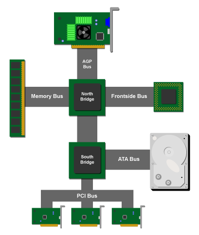
Today's PC architecture comprises a collection of specialized buses with different protocols and bandwidth capabilities. This patchwork of interfaces emerged as the PC industry worked around PCI's limitations by attaching Serial ATA, FireWire, and other bandwidth-intensive interfaces directly to the southbridge. The southbridge has evolved into a versatile I/O hub, continuously adding new interfaces to prevent bandwidth-hungry devices from being starved by the aging PCI bus.
An ideal system would employ a single primary bus and protocol connecting all I/O devices—including the GPU—to the CPU and memory. However, this unified vision remains impractical in the real world and will not materialize even with PCI Express or InfiniBand. Still, the industry requires a way to impose order on this chaos, and that solution has finally arrived in the form of PCI Express.
A primer on PCI
Understanding PCI Express requires first examining how PCI works and where its limitations lie. The PCI bus debuted more than a decade ago operating at 33MHz with a 32-bit width and peak theoretical bandwidth of 132MB/s. As systems demanded more bandwidth, both bus speed and width increased. Later versions offered 64-bit, 33MHz operation with 264MB/s bandwidth, and more recent variants achieved 64-bit, 66MHz performance delivering 512MB/s.
PCI employs a shared bus topology in which all attached devices—network cards, sound cards, RAID controllers, and others—connect to the same bus and communicate with the CPU through it. Since all devices must share this single resource, a bus arbitration scheme determines which device gains access and when, particularly when multiple devices need simultaneous use. Once a device controls the bus, it becomes the bus master, able to communicate with the CPU or memory via the chipset's southbridge.
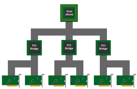
The southbridge, northbridge, and CPU together fulfill the host or root role, which detects and initializes PCI devices while controlling the bus by default. The root's purpose is to connect I/O devices so it can read from them, write to them, and communicate with storage or external systems.
The shared bus topology's main advantages—simplicity, low cost, and ease of implementation—apply only when performance demands remain modest. As requirements increase, the topology's limitations become apparent. From the CPU's perspective, PCI devices appear accessible through a straightforward load-store mechanism using a flat, unified address space dedicated to PCI, resembling main memory address space except that PCI device registers occupy each address range instead of memory cells.
When a PCI-enabled computer boots, the system initializes the PCI subsystem by assigning address space chunks to different devices, making them accessible to the CPU. Once initialized, devices listen to the bus for commands and data directed to their addresses. When a device detects an address it owns on the bus, it reads any following data.
This scheme functions adequately with few devices, but every device listening to the bus injects electrical noise onto it. As more devices attach and listen, noise accumulates, making it progressively harder to maintain a clean signal. This load-related noise phenomenon, combined with clock skew issues, limits PCI buses to five card-based devices maximum. Soldered-on-motherboard PCI devices produce cleaner signals, permitting somewhat higher device counts.
Sharing the bus
The shared bus limitation resembles an office building with a single telephone line that everyone shares. Employees keep their phones off the hook with speakerphones active, listening for the secretary to call their names. With few employees this arrangement proves inconvenient but workable. In an office of hundreds, ambient noise from all speakerphones would render the line unintelligible, making it impossible to hear names called above the cacophony.
When systems require more than five PCI devices, designers must employ PCI-to-PCI bridge chips arranged in a hierarchical tree structure. This tree topology distinguishes PCI from peer-to-peer and point-to-point next-generation interconnects like HyperTransport and InfiniBand. The root at the diagram's top serves as the master controller responsible for initializing and configuring all PCI devices at boot time, making every other PCI device a slave under one master's control. Because the master must enumerate all devices and configure the entire system during startup, hot-plugging and hot-swapping remain impossible.
Organizing bus traffic
Bus traffic divides into two overlapping pairs of categories. The first pair comprises address traffic and data traffic. Data represents the information being sent to or received from an attached device, while address identifies the specific device location or region where information travels. Any multi-device bus requires mechanisms for handling both types and distinguishing between them.
The second pair—command traffic and read/write traffic—overlaps the first. Command traffic consists of configuration or control information sent to a particular device address, encompassing both address and data components. Examples include device initialization instructions, reset signals, and mode-switching commands that allow the CPU to control how PCI devices handle data flow.
Read/write traffic carries the actual information being transmitted to devices. A RAID controller uses read/write traffic to send and receive files from attached hard disks; a sound card uses it to transmit audio data to speakers. Like command traffic, read/write traffic combines addresses with data.
Different buses handle these traffic types differently. Many common bus architectures consist of separate address and data buses, allowing data to flow quickly since each traffic type has dedicated lines. The alternative multiplexes address and data onto a single bus by placing the address first, then following it with data. PCI uses this approach with a single 32-bit bus carrying multiplexed addresses and data. Multiplexing sacrifices some bandwidth efficiency since address traffic consumes space that could carry data, but multiplexed buses cost less than dual-bus designs because they require half the lines and device pins.
Another approach splits traffic into control and read/write categories, assigning each its own bus. This resembles installing a separate management line for supervisors to use when communicating with employees.
PCI and MSI
Later PCI specifications partially adopted the last traffic-handling method, incorporating a "side-band bus"—a smaller bus with dedicated lines for transmitting control and configuration information. However, this side-band bus increases pin count, power consumption, and cost, making it suboptimal.
More recent PCI specifications introduced Message Signal Interrupt (MSI), a method using standard read and write operations to transmit certain command and control traffic to PCI devices. MSI reserves a special message space in the PCI flat memory address space for passing control messages called interrupts. This space functions like a bulletin board where the CPU writes interrupt messages that devices then read. PCI Express expands the MSI specification to include not just interrupts but all side-band control signals.
Summary of PCI's shortcomings
PCI's current implementation suffers from serious limitations preventing it from delivering the bandwidth and features needed by contemporary and future I/O and storage devices. Its highly parallel shared-bus architecture restricts bus speed and scalability, while its simple load-store, flat memory-based communications model lacks the robustness and extensibility of routed, packet-based alternatives.
PCI-X: wider and faster, but still outdated
The PCI-X specification represented an attempt to update PCI with minimal disruption, allowing it to function adequately for several additional years. Consequently, the specification fails to address the inherent problems outlined above and actually exacerbates some of them.
PCI-X essentially doubled bus width from 32 to 64 bits, increasing parallel data transmission capacity and expanding address space. The specification also raised the basic clock rate to 66MHz, with a 133MHz variant available at the high end, further boosting bandwidth to 1GB/s at 133MHz. The latest PCI-X 266 specification double-pumps the bus, transmitting data on both rising and falling clock edges, improving peak theoretical bandwidth, though real-world sustained bandwidth improvements remain more modest.
These improvements significantly increased bandwidth and utility but also raised implementation costs. Faster buses become more sensitive to noise, requiring exceptionally strict manufacturing standards. Poor materials and loose tolerances translate directly into noise at higher speeds, making high-speed PCI-X buses more expensive to manufacture.
The higher clock speed alone does not account for increased noise and manufacturing costs. Increased bus width introduces additional noise through crosstalk as more wires carry signals. Those additional wires connect at their endpoints to multiple PCI devices, increasing electrical load and injecting more noise. Furthermore, PCI devices themselves require 32 extra pins, raising manufacturing costs for individual devices and motherboard connectors.
These combined factors make PCI-X significantly more expensive than PCI, keeping it out of mainstream consumer systems. Most problems associated with increased bus parallelism and double-pumping also affect recent DDR memory variants, particularly DDR-II. Even after addressing these challenges, systems still must contend with PCI's shared-bus topology and its associated problems. Fortunately, a superior alternative exists.
PCI Express: the next generation
PCI Express, formerly known as 3GIO, represents the newest iteration of this technology. Although the PCIe specification was finalized in 2002, market availability of PCIe-based devices has only recently begun. With Intel's launch of its 900-series chipsets and NVIDIA and ATI's announcements of PCIe-compatible cards, PCIe will soon appear in consumer systems.
PCIe's most dramatic improvement over PCI involves its point-to-point bus topology. Unlike PCI's shared bus where devices collectively arbitrate for access, PCIe replaces the shared bus with a central switch serving as the single shared resource through which all devices communicate. Each device gains direct and exclusive access to the switch, sitting on its own dedicated bus—called a link in PCIe terminology.
Like a network router or telephone switchboard, the switch routes bus traffic and establishes point-to-point connections between any two communicating devices. Returning to the office analogy, each employee now has a private line to the front desk; instead of shouting over a shared line, the secretary uses a switchboard to connect employees directly with callers and each other.
In the point-to-point topology, the CPU can communicate with any PCIe device by "dialing" that device's address and opening a direct, private communications link via the switch. Like modern telephone calls or internet connections between browsers and websites, the communicating parties perceive a private, direct, continuous link. In reality, the communications stream breaks into discrete data packets that the switch routes—like a postal worker delivering addressed envelopes—back and forth between parties.
Enabling Quality of Service
The switched fabric topology centralizes the intelligence needed to manage and route traffic in a single chip—the switch. In shared-bus systems, devices must use arbitration schemes to distribute a shared resource among themselves. In switched fabric systems, the switch makes all resource-sharing decisions.
By centralizing traffic routing and resource management functions, PCIe enables an important next-generation capability: quality of service (QoS). The PCIe switch can prioritize packets, allowing real-time streaming packets such as video or audio streams to take priority over less time-critical packets. This should result in fewer dropped frames in first-person shooters and lower audio latency in digital recording software.
Backwards compatibility
PCIe maintains backwards compatibility with PCI, and operating systems can boot and run on PCIe-based systems without modification. This raises the question of how PCI's load-store model can coexist with PCIe's switched packet-based approach. The answer proves straightforward.
Both PCI and PCI Express implement portions of the OSI network stack. While a detailed breakdown of network stacks lies beyond this article's scope, the basic concept is accessible. PCI implements the first four OSI layers, specifying physical transmission aspects from wire-level signals through the higher-level load-store interface that software uses for PCI communication. PCI Express designers preserved this load-store-based, flat memory model unchanged. Legacy applications communicating via PCIe still execute reads from or writes to specific addresses. However, the next two stack levels convert these read or write requests into packets by appending routing, flow control, and CRC information, placing them in frames, and transmitting them to their destinations.
Applications perceive memory address reads and writes when communicating with PCI devices, but behind the scenes, entirely different protocols and signals manage the routing. PCIe converts all PCI side-band signals to MSI signals (which are load-store based) so they can be encapsulated into packets and routed like any other read/write traffic. Consequently, all PCIe traffic types—whether command or read/write, address or data—transmit over a single bus.
Under PCIe, the two pairs of bus traffic types divide logically even if not physically separated onto different buses. Address and data combine in packet form, with the packet core consisting of an address paired with a data chunk. Packets themselves generally fall into two categories: command and read/write. Literature on packet-based bus systems like PCIe or RAMBUS frequently refers to command packets and data packets, with the latter being the more common term for read/write packets.
Traffic runs in lanes
When PCIe designers conceived a true next-generation PCI upgrade, pin count emerged as a critical issue. The earlier PCI section covered problems with large-scale data parallelism—noise, cost, poor frequency scaling—that PCI exhibits. PCIe solves this through a serial approach.
A connection between a PCIe device and PCIe switch is called a link, composed of one or more lanes. Each lane transmits one byte at a time in both directions simultaneously through full-duplex communication, possible because each lane comprises one pair of signals: send and receive.
To transmit multi-byte PCIe packets, a one-lane link must break each packet into a series of bytes and transmit them in rapid succession. The receiving device collects all bytes and reassembles them into a complete packet. This disassembly and reassembly must occur rapidly enough to be transparent to the next stack layer, requiring processing power at each link end. The advantage is that because each lane carries only one byte, very few pins are needed for data transmission. This serial transmission scheme converts processing power into bandwidth, contrasting with PCI's parallel approach that converts bus width and pin counts into bandwidth. Since Moore's Law makes processing power cheaper than bus width, PCIe's tradeoff proves sensible.
A link can comprise "one or more lanes," allowing multiple individual lanes to aggregate into a single link. Two lanes coupled together form a link capable of transmitting two bytes simultaneously, doubling link bandwidth. Four, eight, or more lanes can combine similarly.
A single-lane link is called an x1 link; two lanes form an x2 link; four lanes form an x4 link, and so forth. PCIe supports x1, x2, x4, x8, x12, x16, and x32 link widths.
PCIe's bandwidth gains over PCI prove substantial. A single lane transmits 2.5Gbps in each direction simultaneously. Two lanes combined into an x2 link deliver 5Gbps, with bandwidth scaling accordingly for each link width. These high transfer speeds enable new applications such as SLI video card rendering.
PCIe, the GPU, and you
When announcements of Alienware's new PCIe-based SLI technology circulated, some observers claimed the company had simply rebranded basic PCIe functionality. However, readers who have followed this article's progression will recognize that no single PCIe capability specifically enables this type of video card cooperation. Rather, PCIe's entire high-bandwidth, next-generation package facilitates this functionality, not any individual feature.
3D rendering requires moving substantial data very quickly between the video card, CPU, and main memory. In current systems, the AGP bus represents a significant bottleneck. The amount of RAM vendors cram into high-end video cards demonstrates this bottleneck's severity—all that memory exists so the GPU avoids accessing main memory for rendering data.
PCIe changes this picture dramatically. Two video cards placed in x16 slots gain high-bandwidth pipes connecting them to each other, main memory, and the CPU. They can leverage all that bandwidth to cooperate on rendering tasks at levels previously infeasible with older bus technologies.
Lane negotiation at startup
Observers have noted that no currently available motherboard features two x16 links. Some boards offer two x16 slots, but those slots connect to the bridge via x8 links. This apparent contradiction requires explanation.
At startup, PCIe devices negotiate with the switch to determine the maximum number of lanes the link can support. This link width negotiation depends on the link's maximum width itself (the actual number of physical signal pairs), the connector width into which the device plugs, and the device's width. It also depends on the switch's interface width, though we'll assume the switch's interface width equals the physical link width.
A PCIe-compliant device has a certain number of built-in lanes. NVIDIA's first-generation SLI cards are all x16 cards, meaning they have sufficient copper connectors at their bottom contact edges to support 16 lanes. They must plug into connector slots supporting at least 16 lanes. Fewer lanes would lack sufficient contacts to receive all card signals. More lanes would simply have extra contacts ignored.
However, the card and connector being x16 does not guarantee an x16 link. The physical link itself might have copper traces supporting exactly 16 lanes, fewer than 16, or more than 16. If the link supports fewer than 16 lanes, the switch and device negotiate to determine this, using only available lanes. If the link supports more than 16 lanes, extra lanes are ignored.
Examining a detailed diagram shows how this works: extra lanes are ignored, while insufficient lanes cause devices to throttle bandwidth accordingly. One situation fails completely: plugging an x16 card into an x8 connector does not work because the connector lacks sufficient contacts to receive all card lanes.
This link width negotiation provides flexibility in system design and device integration with different lane widths, but creates consumer-space headaches. Users must match link widths with device widths and will initially find situations confusing where the link width differs from the connector width, such as an NVIDIA card plugged into an x16 slot attached to an x8 link.
An NVIDIA card plugged into an x8 link communicates with the switch, discovers the link's x8 nature, trains down accordingly, and transmits data at the appropriate x8 rate.
PCIe to PCI bridging
Discussions in coming months will frequently mention PCI to PCIe bridging, which fortunately proves simpler to understand than link width negotiation. Essentially, a PCI to PCIe bridge translates PCIe packets back into standard PCI signals, allowing legacy PCI devices to function in PCIe systems. This bridging can occur anywhere from the motherboard to the card itself.
NVIDIA employs this approach with their first-generation PCIe cards, embedding a PCIe-to-PCI bridge directly on the card. This makes the card itself still a "PCI" card despite fitting into a PCIe slot. ATI, by contrast, produces cards supporting PCIe natively and therefore requiring no bridge chip.
These bridges will likely make minimal near-term difference in users' experiences, and will disappear entirely long-term as companies like NVIDIA rework product lines for native PCIe support. The translation chip adds some device cost, but its performance impact (if any) will prove extremely difficult to quantify and impossible to isolate. Nevertheless, expect bridging discussions to feature prominently in graphics industry competition over the coming months. The practical advice is to ignore bridging talk and focus on benchmarks, which represent the only metric that truly matters.
Conclusion: PCI Express in the real world
Intel's new 900-series chipsets exemplify PCIe-to-PCI bridging on the motherboard, incorporating PCIe-to-PCI bridge logic directly into the southbridge. This allows legacy PCI devices to coexist with new PCIe devices within the same system.
Rather than detailing these chipsets in depth—a task already accomplished in available reviews—this article provides one final diagram showing PCIe implementation in newly announced chipsets.
PCIe links extend from both the northbridge and southbridge. Just as the northbridge and southbridge combined with the CPU filled the PCI host or root role, the northbridge and southbridge together fulfill the PCIe switch role. In Intel's design, the north and south bridges function as PCIe switches connected by a single, high-bandwidth PCIe link.
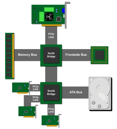
This article opened by discussing how PCI caused different buses to be absorbed into the chipset, with the pre-PCIe chipset functioning as a switch with attached devices resembling a makeshift switched fabric. PCIe brings order to this chaos by transforming the core logic chipset into a genuine PCIe switch. It converts attached buses into PCIe buses and makes the PC as a system more cleanly extensible and future-proof by eliminating the need for successive specialized buses.
Source: Ars Technica