Intel Patent Describes Embedding MicroLEDs Into CPU Packages for Diagnostics and Visual Effects
A newly published Intel patent from 2022 outlines a method for integrating MicroLEDs directly into processor packages, potentially enabling illuminated text displays or decorative lighting on chips themselves.
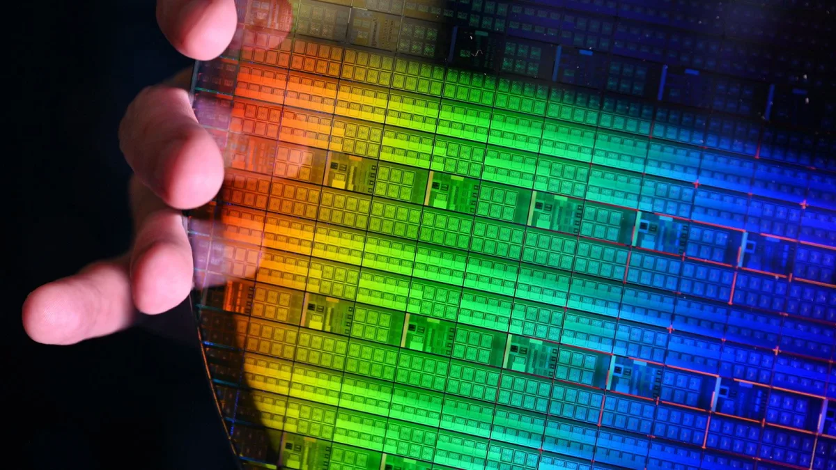
Intel has disclosed a patent for incorporating MicroLEDs into the physical structure of a CPU package, opening possibilities for both functional diagnostics and visual customization. The patent, submitted in 2022 and made public this month, details a technique using a glass substrate and through-glass vias (TGVs) to route power and signals from the MicroLEDs directly to the semiconductor die. According to the filing, these embedded lights would serve "either aesthetic components of the electronic device or to indicate certain operations being performed by the electronic device."
While patents typically leave applications broad and open-ended, Intel's filing specifically focuses on CPU implementation and provides concrete examples of potential uses. The document states that a processor "may operate the micro LEDs so that the micro LEDs visually indicate that certain functions are being performed by the processor or simply for aesthetic effects." One particularly striking application mentioned involves using the LEDs to "light up wording across a central processing unit," suggesting a direct readout capability etched onto the chip surface itself. The practical challenges of displaying such information on a standard processor covered by a heatsink remain unresolved. The patent also emphasizes that the LEDs could emit different colors depending on the design approach, potentially resembling RGB memory lighting or serving as a more functional diagnostic indicator.
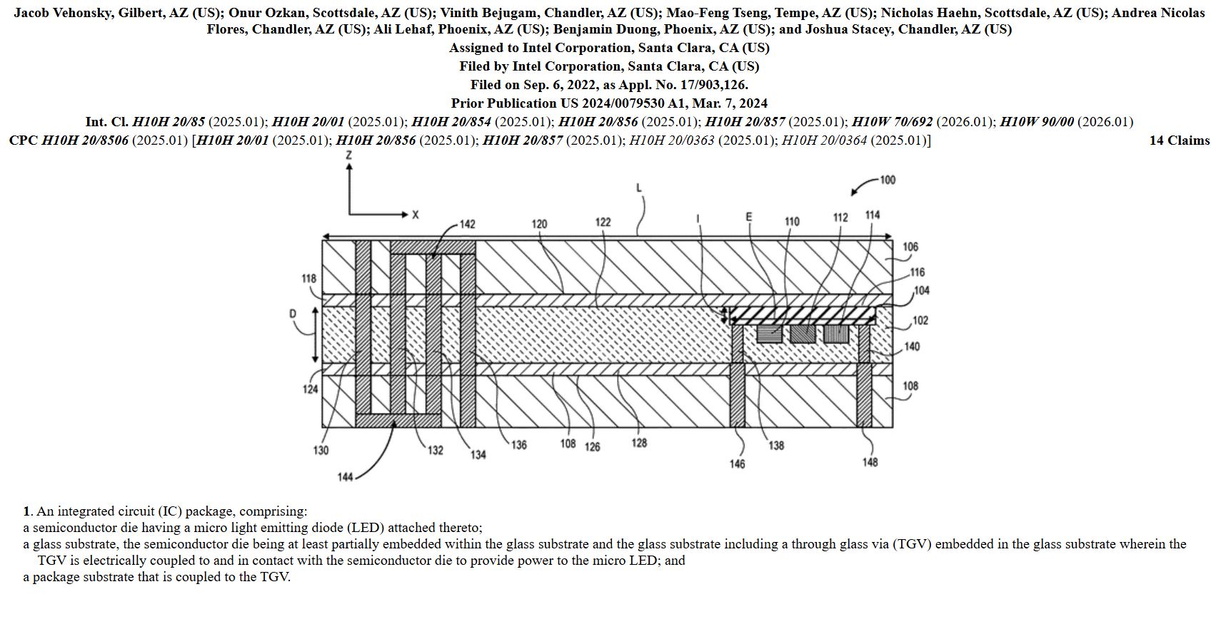
The patent's technical approach positions a glass substrate between two layers of package substrate, with the semiconductor die partially or fully embedded within the glass layer. The MicroLEDs connect to the die either directly or through nanowires, while TGVs supply the necessary power and signals through the glass substrate. Intel specifies that the package incorporates two layers of silicon nitride formed on the substrate surface before attachment to the glass component. The company has invested over three years in glass substrate development, claiming these materials deliver interconnect density roughly ten times superior to conventional organic substrates.
The patent's primary diagram illustrates a single integrated circuit, though the filing notes this representation serves "for clarity" only. A production implementation of this technology would feature "an array or arrays of micro LEDs on one or more IC packages," meaning sufficiently ambitious designs could incorporate multiple LED functions throughout the processor. Still, patents represent potential rather than certainty; Intel filed this particular patent over four years ago, and its recent publication does not guarantee the technology will reach actual products. Whether consumers will eventually see processors with embedded MicroLEDs remains uncertain, though Intel has clearly established the technical foundation for such a development.