Diamond Foundry reaches wafer-scale production with 200mm single-crystal diamond
The lab-grown diamond specialist has created the first 200mm single-crystal diamond wafer, a milestone aimed at solving thermal management challenges in advanced AI processors through diamond's superior heat-dissipation properties.
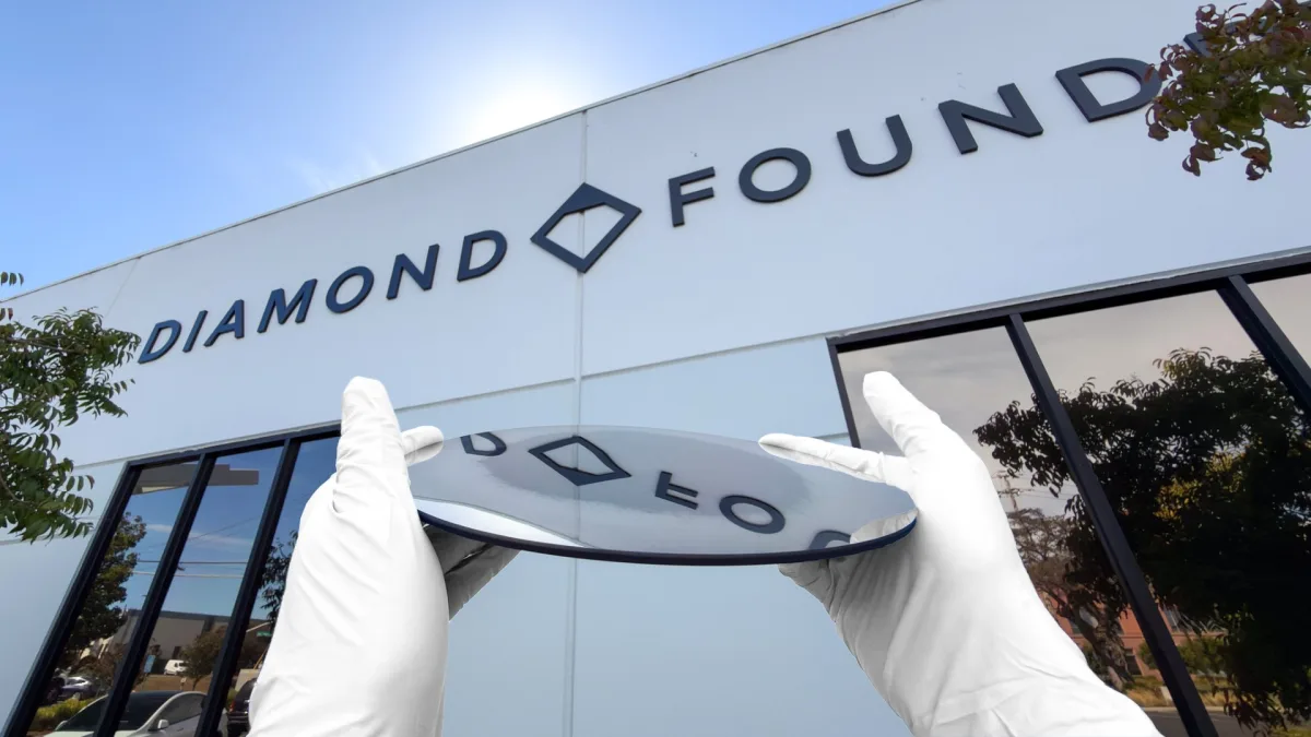
Diamond Foundry, a company specializing in laboratory-produced diamonds, has unveiled what it describes as the industry's first 200mm single-crystal diamond (SCD) wafer. The achievement marks a significant step toward manufacturing diamond at scales relevant to semiconductor production, with the firm declaring on its website that "Single-crystal diamond has entered the wafer-scale era." The 200mm format matches the dimensions of wafers used in legacy semiconductor processes, and the development responds to mounting thermal challenges in high-power artificial intelligence chips.
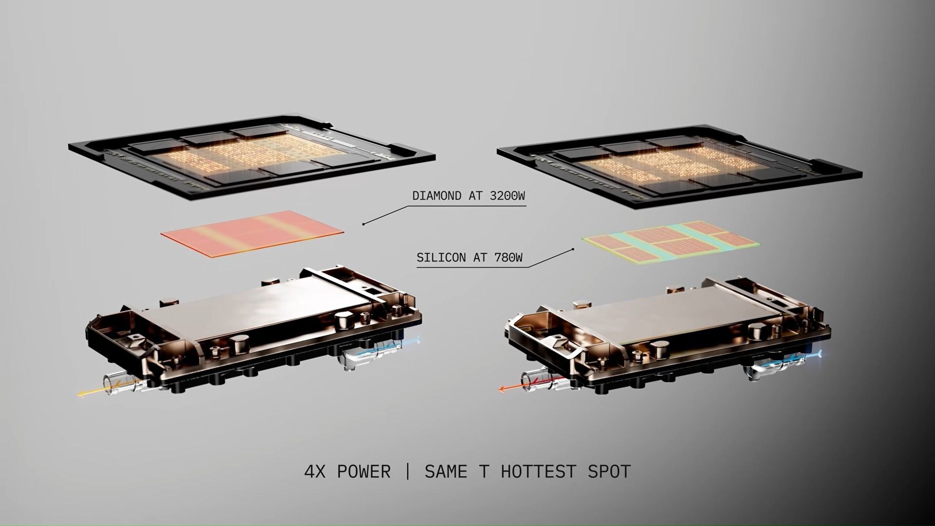
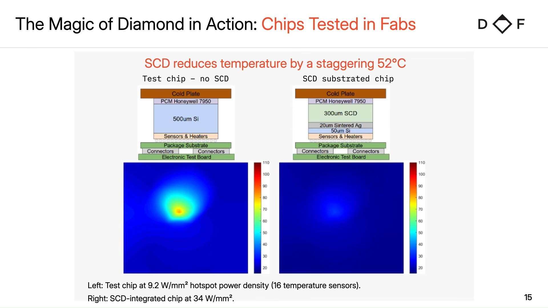
Diamond's thermal properties make it an attractive material for cooling applications. The substance exhibits thermal conductivity estimated to be at least five times greater than copper, positioning it as a potential solution for managing heat in densely packed processor designs. Unlike polycrystalline lab-grown diamonds, Diamond Foundry's wafer is manufactured as a single-crystal structure, a technically demanding process that preserves both the material's thermal efficiency and its electrical insulating characteristics. This combination of properties could reduce the formation of hotspots on AI processors.
The company has projected that a D300 SCD wafer—matching the size used in cutting-edge semiconductor manufacturing—could be feasible before 2030. The sample demonstrated by Diamond Foundry remains unpolished, indicating additional processing steps will be necessary before chipmakers can integrate the material into production workflows.
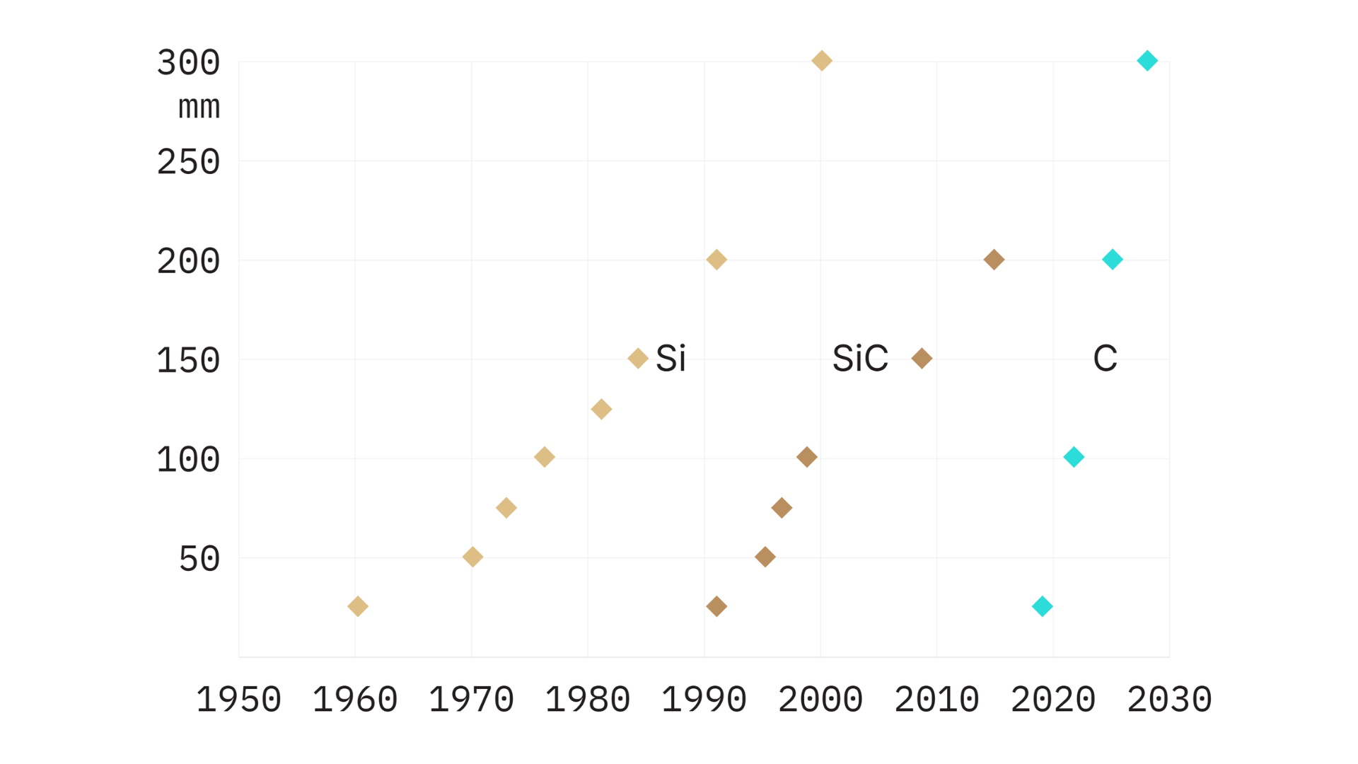
Diamond Foundry, established in 2012, acknowledged the contributions of researchers who have worked on scaling single-crystal diamond production since the early 2000s. CEO Martin Roscheisen commented on the achievement: "This is one of those milestones that once seemed almost impossible. Hundreds of DF engineers, scientists, and technicians contributed to us getting here. It is the accumulated result of countless experiments, failures, inventions, rebuilt machines, and insights over more than a decade."
An unnamed source added perspective on the long-term effort behind the breakthrough: "Stefan and Martin pursued this goal for 25 years. There are very few examples in technology of someone sticking to a really hard scientific challenge with that level of perseverance. They kept going when the prevailing view was that single‑crystal diamond simply could not be made at this scale. Today, the perseverance shows as the first-ever D200mm single‑crystal diamond. And best of all, it makes D300mm predictable as well."
Diamond Foundry is not alone in exploring synthetic diamond for semiconductor thermal management. Akash Systems received $18.2 million in CHIPS Act funding during 2024 to develop Gallium Nitride bonded with synthetic diamond, claiming the combination can reduce temperatures by 20 degrees Celsius. De Beers Group, traditionally known for African diamond mining operations, is developing a copper-plated diamond composite material targeting cooling improvements for artificial intelligence systems, high-performance computing platforms, and GaN RF devices. Frore Systems, recognized for its solid-state cooling technology, is also pursuing diamond-enhanced watercooling cold plates intended for Nvidia's forthcoming artificial intelligence GPU generations.