TSMC Targets 2030 for High-NA EUV Rollout, With A10 or A11 in Focus
Taiwan's chipmaker has broken years of silence on its High-NA EUV plans, committing to deploy the advanced lithography technology by 2030 and laying out a multi-year roadmap for larger photomasks.
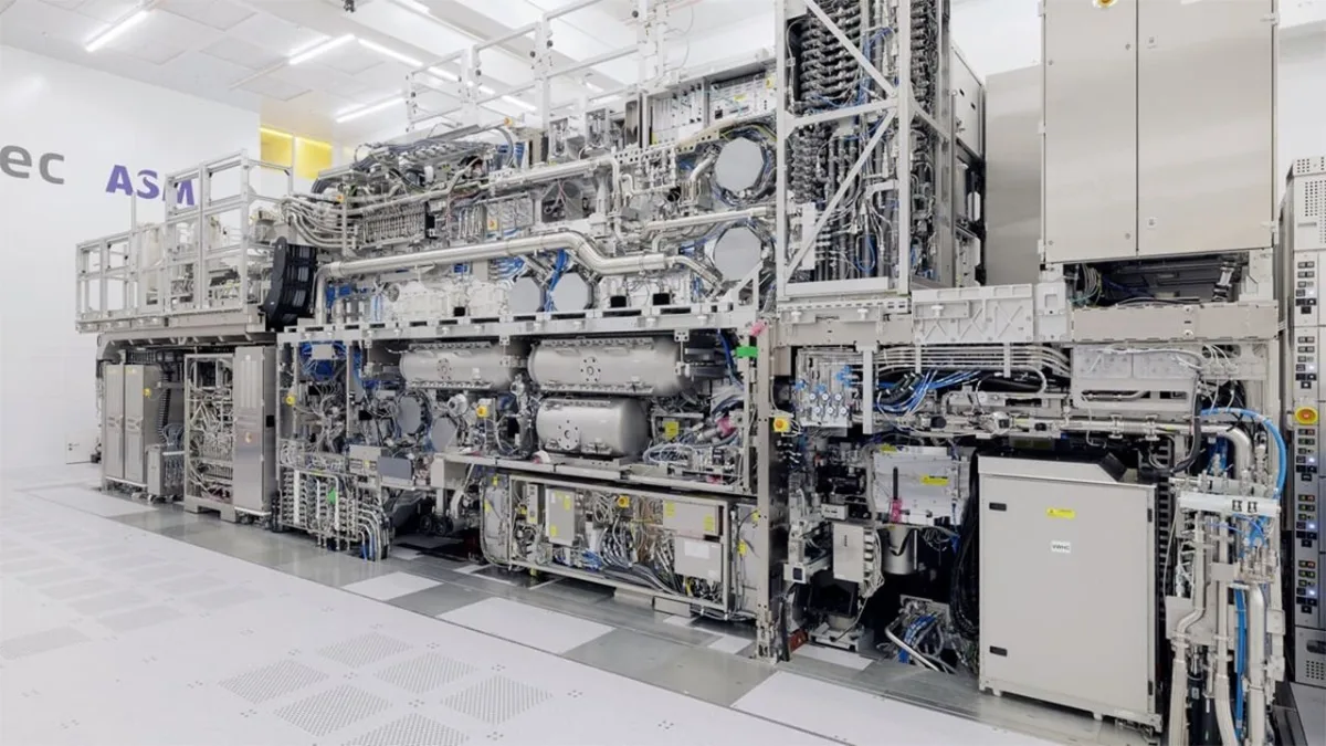
Which node comes first?
For an extended period, TSMC maintained silence regarding its intentions to deploy High-NA EUV lithography, which relies on 0.55 numerical aperture optics, largely because its engineering teams had developed viable pathways to continue advancing chip processes without investing in $400 million scanner systems. Yet the company recognizes it cannot indefinitely depend on Low-NA EUV equipment, prompting an announcement this week of plans to introduce High-NA EUV technology starting in 2030.
The chipmaker has not publicly identified which specific process node will be the inaugural user of High-NA EUV, though the 2030 timeline narrows the field considerably. TSMC indicated that as its process nodes grow increasingly intricate, the proportion of layers utilizing High-NA EUV will expand accordingly. This expansion likely reflects growing sophistication in transistor design, including potential advances in gate-all-around (GAA) architectures and complementary field-effect transistors (CFETs) in subsequent generations.
According to TSMC's timeline, High-NA EUV lithography equipment will enter high-volume manufacturing in 2030 using standard 6×6-inch photomasks. The company intends to establish a test facility in 2031 that operates with 6×12-inch photomasks, with the objective of transitioning 6×12-inch High-NA systems into production for advanced nodes by 2033.
The photomask challenge
High-NA EUV systems can achieve 8nm single-pass resolution, compared to the 13nm capability of current Low-NA EUV equipment. However, when paired with conventional 6×6-inch photomasks, High-NA EUV scanners deliver only half the exposure area of their Low-NA equivalents, creating complications for manufacturing oversized processors. Consequently, companies developing large AI chips face a choice between stitching multiple exposure regions or embracing chiplet-based architectures, each approach introducing distinct manufacturing and operational trade-offs. TSMC is collaborating with ASML to enable the transition to 6×12-inch photomasks as a solution.
Transitioning photomask dimensions represents a substantial undertaking, necessitating modifications across design software, mask production equipment, mask writing systems, and mask handling infrastructure—essentially requiring industry-wide coordination. ASML has expressed confidence in this transition, backed by commitments from Intel, TSMC, and Samsung.
We expect the adoption of High NA EUV to increase progressively along the device scaling roadmap, first using current 6-inch masks and then further supported by 12-inch masks, which enable greater scanner productivity and allow the industry to meet the demand for smaller, faster and more energy-efficient chips. We are pleased by the strong initial support of semiconductor manufacturers, mask suppliers and partners for this initiative.
Christophe Fouquet, president & CEO, ASML
A10 or A11 as leading contenders
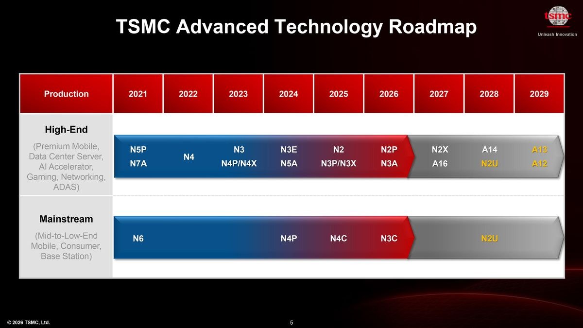
The most compelling question surrounding TSMC's High-NA EUV deployment concerns which process generation will pioneer the technology. Examining TSMC's publicly disclosed roadmap, the A10 or A11 (representing the 1/1.1nm class) emerge as the most probable candidates for deploying High-NA EUV systems on the most demanding layers. TSMC's approach divides its roadmap into yearly client-focused nodes (N2, N2P, N2X, A14, A13) and roughly two-year-cycle high-performance nodes (A16 launching in 2027, followed by A12 in 2029). The company has already stated that both A12 and A13, scheduled for 2029, will maintain reliance on conventional EUV lithography.

Given that A13 represents an optical refinement of A14 with only a 6% boost in transistor density and undisclosed performance and efficiency gains, its successor arriving in 2030 will likely require substantially more significant improvements. Therefore, A13's follow-on—potentially designated A11 or A10—should incorporate either more sophisticated lithography techniques and/or TSMC's third-generation nanosheet GAA transistors to achieve meaningfully higher transistor density alongside substantial performance and efficiency advances relative to A13. These remain educated assessments rather than confirmed information.
Source: Tom's Hardware