Raspberry Pi Slashes Defect Returns in Half With Manufacturing Process Overhaul
By switching to intrusive reflow soldering in partnership with Sony, Raspberry Pi has dramatically reduced product returns while speeding up production and cutting carbon emissions.
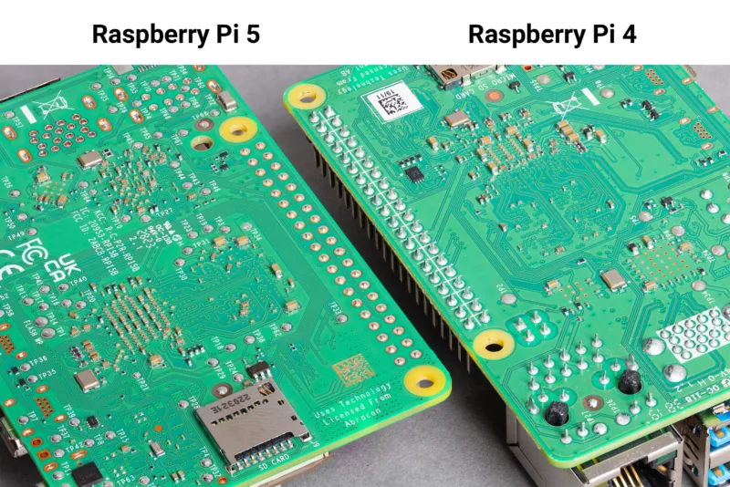
Mastering through-hole soldering presents genuine challenges for hobbyists working with basic equipment at home. Yet it turns out that the technique posed equally significant manufacturing hurdles for a company responsible for producing more than 60 million units. Raspberry Pi boards combine surface-mount devices (SMDs) with through-hole components, each requiring different assembly approaches.
Surface-mount technology enables manufacturers to attach numerous small components—chips, resistors, and other elements—using tiny pins, flat contacts, or solder balls. Larger parts or those exposed to physical stress, such as connectors handled by users, still depend on through-hole soldering, where leads pass through holes and receive solder to form secure joints.
The Raspberry Pi board features a 40-pin GPIO header requiring through-hole soldering, alongside components like Ethernet and USB ports that demand robust connections. These parts cannot be processed using standard surface-mount methods. "In the early days of Raspberry Pi, these parts were inserted by hand, and later by robotic placement," explains Roger Thornton, director of applications for Raspberry Pi, in a blog post. Following placement, boards underwent a separate wave soldering stage.
The manufacturing process has evolved significantly. Raspberry Pi now solders both small and large components simultaneously through intrusive reflow soldering, executed in collaboration with the company's UK manufacturing partner, Sony. By fine-tuning component positioning, adjusting the solder stencil, and modifying connectors, manufacturers can now complete all assembly steps in a single operation.
https://www.youtube.com/embed/obYHpjzhyAw?start=0&wmode=transparent
Intrusive reflow soldering applies solder paste to pads designated for SMD components and directly into through-hole pin locations. Through-hole parts are positioned onto the paste, and the entire board enters a reflow oven where heat melts the paste, allows connectors to settle fully, and creates solder joints for both SMD and through-hole components simultaneously.
While intrusive reflow soldering itself is not a novel technique, its implementation at Raspberry Pi has delivered measurable results. According to Thornton, the company achieved "a massive 50% reduction in product returns." The shift also accelerated manufacturing by 15 percent by eliminating the interval between two separate soldering operations. Removing the distinct soldering bath from production also lowered annual carbon dioxide emissions by 43 tonnes per year (or 47.4 US tons).
The specifics of the 50 percent reduction—whether comparing Raspberry Pi 5 to Raspberry Pi 4, or whether it encompasses all returns or only board defects—remain unclear. Regardless, the achievement underscores a meaningful advancement in manufacturing efficiency and provides additional motivation for those considering the upgrade from hand soldering to paste and stencil methods.
Source: Ars Technica